Home Koala Gallery Download Services Purchase Contact
Semiconductor and MEMS structures are difficult to visualize for even the most seasoned EDA professional - and ever-increasing design and fabrication process complexity compounds the issue daily. Editor screen-shots or simple 3d GDSII views are no longer enough to capture the full complexity of your design structures.

From sober engineering diagrams to eye-catching multitextured full-perspective displays, from plan views of routing to cut-aways deep into the substrate, Koala blows away problems of scale and complexity by presenting your designs in eye-catching fluidly animated 3D.

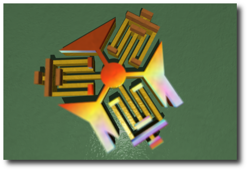
MEMS with Diffraction

Sample 3D GDSII Cell Structures
One of a series of an experimental design for the NIST Nanosoccer Competition. Although at this physical scale optical diffraction effects are not possible as shown (the device is around 320 by 320 microns), diffraction adds a level of interest to the image which is guaranteed to catch viewers attention.

The GDSII for this structure was created by Calin Plesa, who has an tutorial on his blog at calin.nems.ca.


Copyright 2004 - 2009 David Carron.      Contact Us | Terms of Use | Site Map |  Privacy Policy